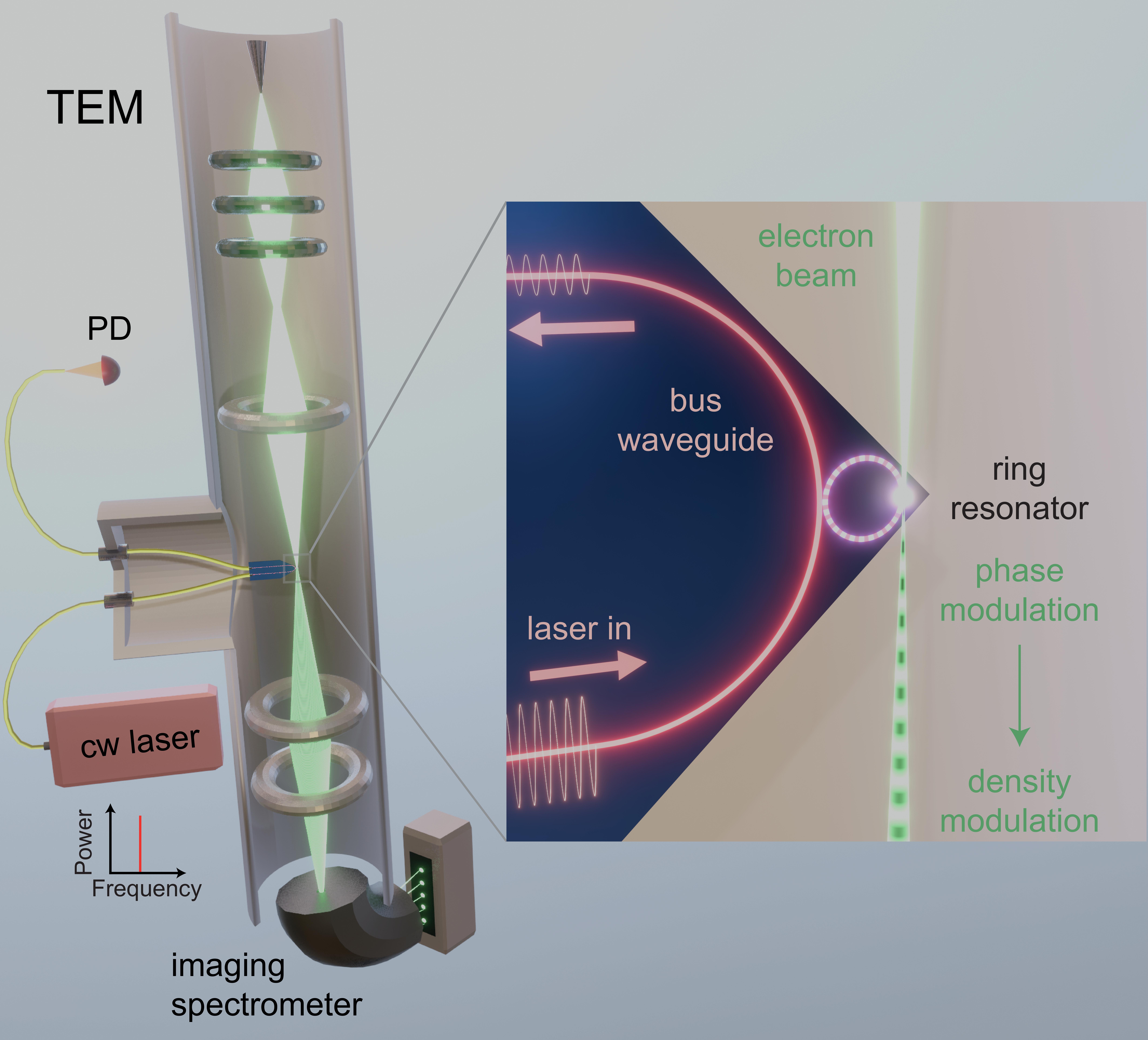
The transmission electron microscope (TEM) can image molecular structures at the atomic scale by using electrons instead of light, and has revolutionized materials science and structural biology. The past decade has seen a lot of interest in combining electron microscopy with optical excitations, trying, for example, to control and manipulate the electron beam by light. But a major challenge has been the rather weak interaction of propagating electrons with photons.
In a new study, researchers have successfully demonstrated extremely efficient electron beam modulation using integrated photonic microresonators. The study was led by Professor Tobias J. Kippenberg at EPFL and by Professor Claus Ropers at the Max Planck Institute for Biophysical Chemistry and the University of Göttingen, and is published in Nature.
The two laboratories formed an unconventional collaboration, joining the usually unconnected fields of electron microscopy and integrated photonics. Photonic integrated circuits can guide light on a chip with ultra-low low losses, and enhance optical fields using micro-ring resonators. In the experiments conducted by Ropers’ group, an electron beam was steered through the optical near field of a photonic circuit, to allow the electrons to interact with the enhanced light. The researchers then probed the interaction by measuring the energy of electrons that had absorbed or emitted tens to hundreds of photon energies. The photonic chips were engineered by Kippenberg’s group, built in such a way that the speed of light in the micro-ring resonators exactly matched the speed of the electrons, drastically increasing the electron-photon interaction.

The technique enables a strong modulation of the electron beam, with only a few milli-Watts from a continuous wave laser – a power level generated by a common laser pointer. The approach constitutes a dramatic simplification and efficiency increase in the optical control of electron beams, which can be seamlessly implemented in a regular transmission electron microscope, and could make the scheme much more widely applicable.
“Integrated photonics circuits based on low-loss silicon nitride have made tremendous progress and are intensively driving the progress of many emerging technologies and fundamental science such as LiDAR, telecommunication, and quantum computing, and now prove to be a new ingredient for electron beam manipulation,” says Kippenberg.
“Interfacing electron microscopy with photonics has the potential to uniquely bridge atomic scale imaging with coherent spectroscopy,” adds Ropers. “For the future, we expect this to yield an unprecedented understanding and control of microscopic optical excitations.”
The researchers plan to further extend their collaboration in the direction of new forms of quantum optics and attosecond metrology for free electrons.
The silicon nitride samples were developed in the Center of MicroNanoTechnology (CMi) at EPFL. The experiments were conducted at the Göttingen Ultrafast Transmission Electron Microscopy (UTEM) Lab.Financement
Deutsche Forschungsgemeinschaft (DFG)
Air Force Office of Scientific Research (AFOSR)
Swiss National Science Foundation (SNF)
European Union Horizon 2020 (EBEAM, SEPhiM)Références
Jan-Wilke Henke, Arslan Sajid Raja, Armin Feist, Guanhao Huang, Germaine Arend, Yujia Yang, F. Jasmin Kappert, Rui Ning Wang, Marcel Moeller, Jiahe Pan, Junqiu Liu, Ofer Kfir, Claus Ropers, Tobias J. Kippenberg, “Integrated photonics enables continuous-beam electron phase modulation”, Nature, 23 December 2021. DOI: 10.1038/s41586-021-04197-5
Auteurs: Arslan Raja, MPI , Nik Papageorgiou
Source: Sciences de Base | SB
